current location :home>News
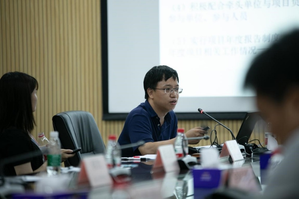
At 14: 00 on July 11, 2019, the Project Kick-off Meeting of Key Technology Research and Application for GaN Power Devices on Si Substrates was held in Conference Room 114, Taizhou Building of Southern University of Science and Technology. Mr. Wei Wenqiu, representative of the Department of Science and Technology of Guangdong Province, Professor Li Shuti of South China Normal University, Professor Jiang Hao of Sun Yat-sen University, Mr. Chen Wenxian of the Electronic Information Technology Department of Shenzhen Science and Technology Innovation Commission, Dean Yu Hongyu and Vice Dean Zhou Shengming of the School of Microelectronics, representatives of partners for this project as well as professor representatives of the School of Microelectronics attended the kick-off meeting. The meeting was hosted by Mr. Lu Min of the School of Microelectronics.

Mr. Wei Wenqiu speaks
Mr. Wei Wenqiu of the Department of Science and Technology of Guangdong Productivity Promotion Center first introduced the conditions and management procedures for key research and development programs of Guangdong Province in 2019. He made it clear that the purpose of this kick-off meeting is to "learn policies, build mechanisms, and ensure implementation". He introduced the relevant management procedures of key research and development programs, as well as clarified the missions and responsibilities of different parties.

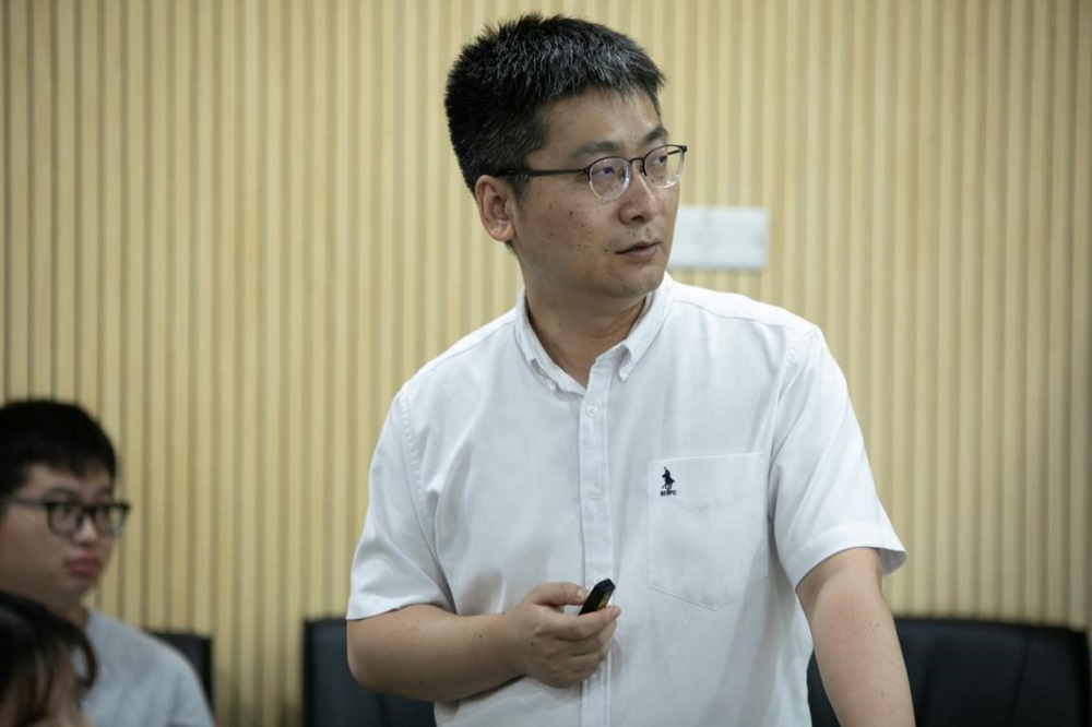
Professor Yu Hongyu speaks
Professor Yu Hongyu, Dean of the School of Microelectronics gave a brief introduction of the school, which has been officially approved as a preparatory school of the "national exemplary school of microelectronics". In the early construction of the school, various tasks were carried out in an orderly and rapid way, and good results were achieved in talent introduction, student training and IUR cooperation.
The Southern University of Science and Technology and 9 participants of the project introduced the preliminary foundation, division of labor, current progress and future work plan of the project.
The evaluation experts put forth valuable opinions and suggestions for the project,considering that all parties of the project should be fully equipped and have reasonable members paying attention to the integrity of internal cooperation of the project. It was hoped that this project will realize the internal circulation of extension, chip design, process flow, device testing and packaging to circuit driver module and realize self-production. At the round table, everyone enthusiastically voiced their suggestions on the project and their outlook on the next work plan.
The Project Kick-off Meeting of Key Technology Research and Application for GaN Power Devices on Si Substrates was Held Successfully. This project, following the energy-saving application requirements of the state and Guangdong Province, carries out the R&D of Si-based GaN enhanced power switch tubes with independent intellectual property rights on the 6-inch product line to solve the key technical problems of Si-based GaN, including large-size high-voltage epitaxy, industrial preparation, reliability, high-frequency drive chips and DC-DC modules, realizing the coordinated innovation of the whole industrial chain and promoting the application process of GaN in the field of high-efficiency power supply.
