current location :home>Research

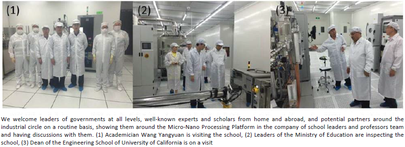
This platform consists of a complete set of advanced equipment, ranging from NanoBeam electron beam exposure machine to SUSS contact-type ultraviolet exposure machine with SUSS automatic gluing machine; the coating equipment consist of Picosun atomic layer deposition (ALD), Lesker multi-source integrated sputtering apparatus, electron beam evaporation and double cavity magnetically controlled sputtering device; the etching equipment consist of inductively coupled plasma (ICP) etching machine of North Microelectronics, and Chuangshiweina RIE equipment. Besides, there are rapid thermal processing furnace (RTP), LPCV furnace tube, muffle furnace, rinsing table, gumming machine, baking oven and other processing equipment. Gauging equipment consists of ellipsometer, desktop SEM, 4 probes and eTester, etc.
This micro-nano processing platform is technically advanced as it has functions likethin film deposition, photoetching, etching, and integrated processing. The processing equipment and technologies of this micro-nano processing platform can be used in (1) development and research of advanced electronic devices on the micro-nano scale; (2) processing of various sensors and MEMS; (3) R&D of the third generation of semiconductor power devices; (4) novel low-dimension electronic materials development at atomic level and its production, and so forth.
The goal is to cultivate entrepreneurial talents and corporate leaders in the microelectronics industry, and to build a world-class industry-university-research transformation platform.


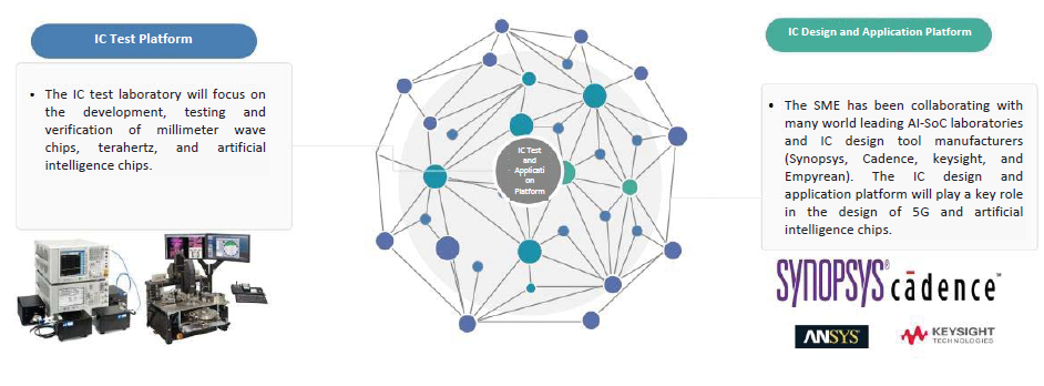
The IC Design, Test and R&D Platform is the foundation to support the design of high-end integrated circuit chips and devices. By building a world-class IC design and test platform, the SME aims at several research directions with urgent industrial needs or major scientific research influences, including millimeter wave chips, terahertz, artificial intelligence chips, and is carrying out equipment capacity planning and construction, striving to make prominent achievements in the short term (within 2-3 years).

The Engineering Research Center on Future Communication IC Sponsored by the Ministry of Education (Abbreviated as the Future Communication IC Engineering Center; Website: https://moecenter.sme.sustech.edu.cn/), it is an engineering research center sponsored by the Ministry of Education focusing on the field of future communication (such as 5G, 6G, etc.) IC. The School of Microelectronics and Cutting-edge and Cross-science Research Institute take the lead to build the center based on Southern University of Science and Technology. The Future Communication IC Engineering Center plans to invest 20 million yuan. Guided by the national science and technology development planning, it will accurately meet China's strategic demands of "Driving 5G development with innovation and breaking through key core technologies", and focus on research of the next generation communication system applicable to the key common technologies of IC suitable for current 5G and future communication applications (such as gallium nitride core devices / CMOS PA / amplifiers, ADCs / filters, etc.)
As an important part of the scientific and technological innovation system of South University of Science and Technology, the center will take "Independent Innovation Leads to Advanced Position" as the goal to carry out research on the basic and key technologies in three key fields: future communication IC design, intelligent storage and computing integration, wide band gap semiconductor materials and devices, intelligent storage and computing integration, and advanced IC manufacturing technology and sensors, and cooperate with leading enterprises such as Huawei and ZTE to achieve technological breakthrough and achievement transformation and cultivate high-end talents required by the industry.
Meanwhile, the Future Communication IC Engineering Center will also effectively strengthen the in-depth cooperation and resource sharing among the departments of South University of Science and Technology, promote the intersection of branches of learning, promote the construction and common development of various branches of learning, and actively build an exchange and cooperation platform for well-known universities in the Greater Bay Area, including Hong Kong University of Science and Technology, the University of Hong Kong, Hong Kong Polytechnic University and the University of Macau, etc. It aims to become a dual driving engine for technological innovation and talent training in the field of future communication core technology, so as to provide strong support for the rapid development of China's future communication.
The GuangDong 3-D Lab is one of the first 6 engineering research centers approved by GuangDong Development and Reform Commission. Established in 2021, it is led by Southern University of Science and Technology (SUSTech) and jointly built by Shennan Circuit Co., LTD, Institute of Semiconductors of Guangdong Academy of Sciences and others. The Lab will target the major needs of China and IC industry, and carry out near-production R&D on 3-D integration.(Please visit the website of the Engineering Center to learn more; Website: http://3dic.sme.sustech.edu.cn/)