current location :home>Research
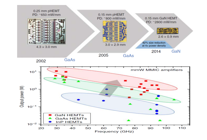
Gallium Nitride RF Device
The goal is to realize RF GaN HEMT devices with high frequency, high power and low loss, which are mainly used in power amplifiers.
Develop power amplifier Gan devices suitable for 5G band and Sub-6G band, mainly research: (1) ohmic contact, (2) gate structure, (3) surface passivation, etc.
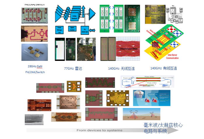
Wireless Communication Chip
The goal is to realize small base station of 5G millimeter wave and its core communication devices and chips (PA, LNA, Switch, ADC, etc.), and the first 26GHZ GaN power amplifier in millimeter wave band in China has been developed.
Develop 77GHz millimeter wave radar chip and undertake 6G communication projects, such as IC core module of 140GHz communication.
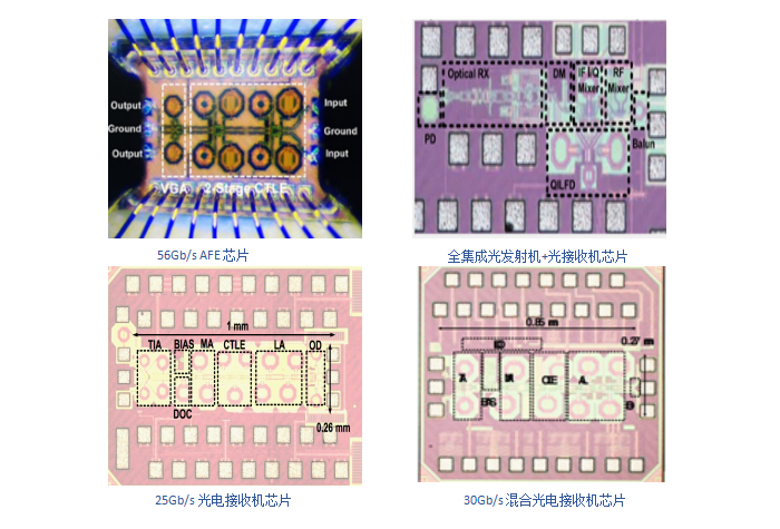
Optical Communication Chip
Optical communication has the advantages of large bandwidth flux, low electromagnetic interference, low dielectric loss, long transmission distance and good confidentiality, etc. Optical communication / photoelectric communication module is widely used in various data centers to meet the requirements of high bandwidth and high rate.
The goal is to realize optical communication chips and components (AFE, TIA, VGA, etc.) with high bandwidth, high rate and low power waste.
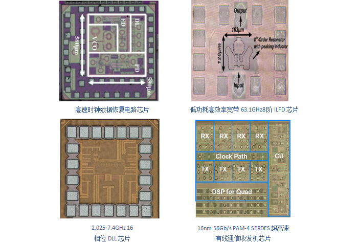
Wired Communication Chip
Wired communication has the advantages of good anti-interference ability, strong reliability and confidentiality, mature technology and stable transmission. It is suitable for medium and short distance signal transmission.
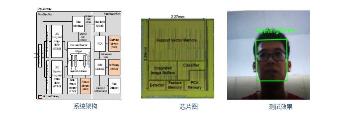
Face Recognition Processor Chip with Low Power Waste
At present, the first near storage-computing architecture based on low power waste SRAM solves the problem of power waste, and the operating power consumption is only 23mW.
TSMC 40nm process, with an area of 2.85x2.27mm2, processes 1280x720 high-definition images in real time at the speed of 5 FPS.
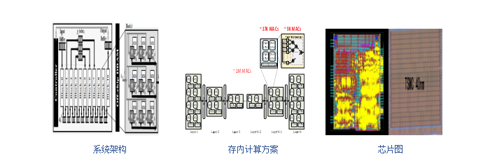
Deep Learning Chip with Low Power Waste, High Flux and Binarization
The first binary deep learning accelerator chip realizes low power waste (30mW) and high flux (2.5TOPS), and the energy efficiency is 7 times higher than that of GPU.
TSMC 40nm process, achieved 34fps scene text image (128 × 32), with an accuracy of more than 90%.
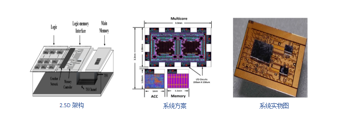
Multi-core Processor Chip with High Flux
It is the first one based on 2.5D interconnection integration process to solve the problem of bandwidth and integrate 16-core H.264 image processor chip to realize 24Gbps bandwidth and 7.5pJ/bit energy efficiency.
TSMC 65nm + TSI process, 2.5D interposer interface provides 8Gbps transmission rate for 12 inter chip interconnected channels.
Tensor Compression Algorithm and Chip
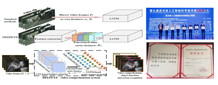
The deep learning network is optimized by tensor compression and training quantization algorithm, and finally forms a deep neural network with high integration, high flux and low power waste, which is suitable for CNN and RNN. It greatly increases the compression rate and reduces the complexity of data processing, and can be realized on a special AI chip on a large scale.
High Dynamic Image Processing ASIC
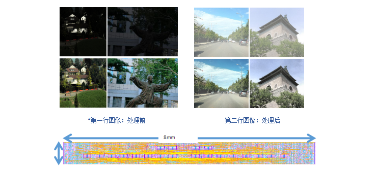
A single frame high dynamic image processing framework is proposed, which is dynamic adaptive histogram equalization based on supervised visibility quantization model.
A pixel-level stream-lined high dynamic image processing ASIC is designed based on 180 nm CMOS process. As a part of the micro display chip (OLEDos), the circuit is used to improve the image quality and form a high dynamic range image. The circuit designs a contrast limited adaptive histogram equalization circuit structure with cumulative distribution function filtering, supplemented by gamma correction and logarithmic correction circuits, which can achieve real-time video image processing and effectively suppress the noise in the image.
Dual-core Object Recognition Coprocessor
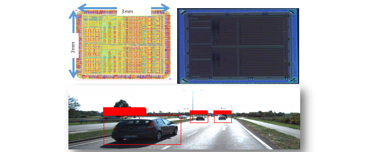
A dual-core object recognition coprocessor with pixel-level stream-lined for image feature extraction is designed based on 65 nm SOI CMOS process. The feature space includes Histogram of Oriented Gradients and Haar-like features.
It is applied to pedestrian, automobile and other target recognition and local feature recognition. In the process of feature extraction, the image sensor data can be processed synchronously, so the memory for temporarily storing one or more frame images and integral images is avoided.

![]() Gallium Nitride Photoelectric Sensor
Gallium Nitride Photoelectric Sensor
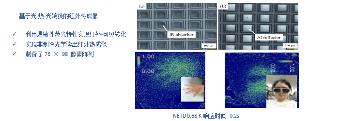
![]() Infrared Detection Sensor
Infrared Detection Sensor
In-vitro Diagnostic Chip
