current location :home>News
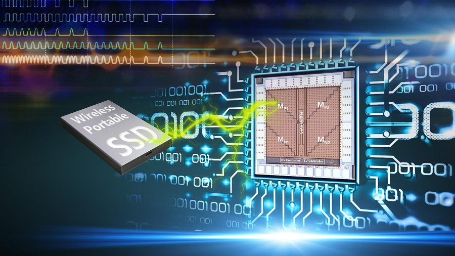
Recently, Dr. Chenchang Zhan, Associate Professor of the School of Microelectronics at the Southern University of Science and Technology (SUSTech), and Dr. Yan Lu, Associate Professor of the Faculty of Science and Technology at the University of Macau (UM), have made significant progress in the field of wireless power transfer (WPT) chip design, an important area of power management IC research. Their Ph.D. student Jie Lin, jointly supervised by the two parties, successfully developed a 6.78MHz single-stage single-output WPT receiver with an ultra-fast transient response, and a high-efficiency single-stage dual-output rectifier also with fast-response and used in WPT.

The afore-mentioned research outputs were published in the IEEE Transactions on Power Electronics (TPEL), which is a top journal in the field of power electronics, entitled "A 6.78-MHz Single-Stage Wireless Power Receiver with Ultra-Fast Transient Response Using Hysteretic Control and Multi-Level Current-Wave Modulation", and "A Single-Stage Dual-Output Regulating Rectifier With Hysteretic Current-Wave Modulation" in the top journal in the integrated circuit design field, the IEEE Journal of Solid-State Circuits (JSSC) (hereinafter referred to as "Paper 1" and "Paper 2").
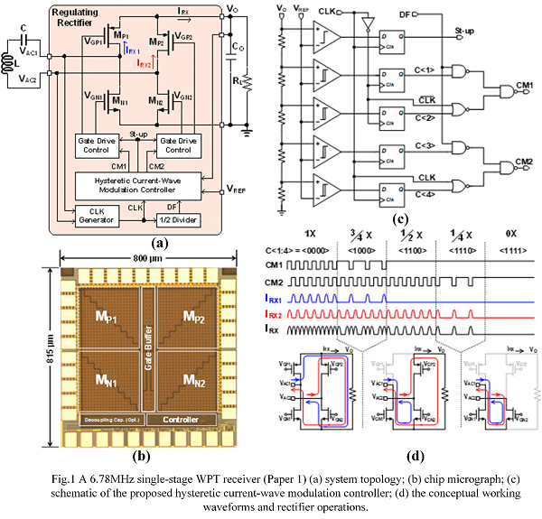
WPT has been widely used in mobile devices such as smartphones and it provides a convenient way of power charging. However, the conventional WPT receiver requires multiple stages (i.e., AC-DC and DC-DC conversions) to achieve a complete function, which will cause the system to occupy a large chip area, use many off-chip components, and result in low conversion efficiency and slow transient responses. To mitigate these problems, the research team developed hysteresis control and multi-level current wave modulation (Multi-level CWM) techniques to achieve the single-stage voltage regulation and fast transient response in Paper 1.
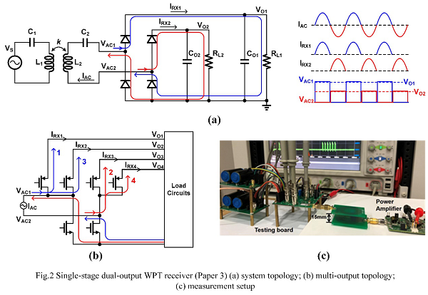
In Paper 2, the system is further improved, and a single-stage dual-output topology is proposed. The input AC voltage waveform is divided into two half-waves to supply power to the two loads, and two independent three-level current wave modulators (3-level CWM) realize the voltage conversion and output voltage regulation. At the same time, the paper expands the situation to N-output, with only N+2 power transistors needed to support N-output conditions. Both of the above two chips are implemented utilizing a standard 0.18μm 1.8-/3.3-V CMOS process. Measurement results show that Paper 1 achieves a peak efficiency of 92.14% and when the load current steps between 12mA and 600mA, there is no noticeable undershoot/overshoot in the output voltage.
Therefore, in Paper 2, the dual output of 1.8V and 3.3V is realized. When the output current is 200mA, the efficiency reaches 91.9%, and it also performs well in terms of load transient response and output cross-regulation. Compared with the state-of-the-art designs, the two chips achieved the world’s best-level performances in terms of chip area, power efficiency, and load transient response among other performance metrics.


The single-stage fast-response WPT receiver in Paper 1 has also been reported as an oral presentation at a top international conference, i.e., the 2020 IEEE Asian Solid-State Circuits Conference (A-SSCC) (refer to the link below for further details). Furthermore, the research team applied for two pending Chinese patents on the dual-output and multi-output WPT receivers proposed in Paper 2.
Ph.D. student Jie Lin at SUSTech is the first author of the above-mentioned papers and inventor of the pending patent. JSSC is generally considered to be the highest-level journal in the field of semiconductor chip design, and its academic influence is comparable to that of Nature and Science in the broader scientific field. Dr. Chenchang Zhan and Dr. Yan Lu are the co-corresponding authors of the papers.
Related Links:
Paper 1: https://doi.org/10.1109/TPEL.2021.3062400
Paper 2: https://doi.org/10.1109/JSSC.2021.3071221
Oral Report: https://doi.org/10.1109/A-SSCC48613.2020.9336129